| Citation: |
E.M. Darivianaki, M. Androulidaki, K. Tsagaraki, M. Kayambaki, G. Stavrinidis, G. Konstantinidis, E. Dimakis, N. T. Pelekanos, C. C. Stoumpos. Hybrid perovskite/GaAs nanowire diodes[J]. Materials Lab, 2025, 4(3): 250005. doi: 10.54227/mlab.20250005

|
Hybrid perovskite/GaAs nanowire diodes
-
Abstract
Halide perovskites have dominated the field of photovoltaics in the past decade with record-breaking efficiencies demonstrated very recently. Likewise, III-V semiconductors represent the state-of-the-art in photovoltaics, being the model system of photovoltaic structure engineering. Herein, we investigate the possibility of using GaAs as an Electron Transporting Layer (ETL), substituting conventional ETLs in halide perovskite photovoltaics. We demonstrate our hypothesis on hybrid CH3NH3PbI3 perovskite/GaAs nanowire (NW) heterostructures, specifically choosing GaAs in its NW form to enhance the electrical contact area between the two materials. The thus obtained heterostructures exhibit a characteristic diode response with improved electrical characteristics when n-doped GaAs NWs are employed. These initial results, which are promising in terms of III-V/perovskite heterojunctions, can potentially lead to efficient CH3NH3PbI3/GaAs NW photovoltaics.
-

-
References
1. H. Min, D. Y. Lee, J. Kim, G. Kim, K. S. Lee, J. Kim, M. J. Paik, Y. K. Kim, K. S. Kim, M. G. Kim, T. J. Shin, S. Il Seok, Nature, 2021, 598, 444 2. A. D. Taylor, Q. Sun, K. P. Goetz, Q. An, T. Schramm, Y. Hofstetter, M. Litterst, F. Paulus, Y. Vaynzof, Nat. Commun., 2021, 12, 1878 3. M. Saliba, T. Matsui, J. -Y. Seo, K. Domanski, J. -P. Correa-Baena, M. K. Nazeeruddin, S. M. Zakeeruddin, W. Tress, A. Abate, A. Hagfeldt, M. Grätzel, Energy Environ. Sci., 2016, 9, 1989 4. M. Lyu, S. Park, H. Lee, B. S. Ma, S. H. Park, K. -H. Hong, H. Kim, T. -S. Kim, J. H. Noh, H. J. Son, N. -G. Park, ACS Appl. Mater. Interf., 2021, 13, 35595 5. National Renewable Energy Laboratory, Photovoltaic Research. https://www.nrel.gov/pv/cell-efficiency , July 2024. 6. Z. Li, T. H. Kim, S. Y. Han, Y. -J. Yun, S. Jeong, B. Jo, S. A. Ok, W. Yim, S. H. Lee, K. Kim, S. Moon, J. -Y. Park, T. K. Ahn, H. Shin, J. Lee, H. J. Park, Adv. Energy Mater., 2020, 10, 1903085 7. J. Wang, P. Zhao, Y. Hu, Z. Lin, J. Su, J. Zhang, J. Chang, Y. Hao, Solar RRL, 2021, 5, 2100121 8. J. O. Akinlami, A. O. Ashamu, J. Semicond., 2013, 34, 03200 9. Y. Sun, L. Liu, Z. Lv, X. Zhangyang, F. Lu, and J. Tian, Mater. Sci. Semicond. Proc., 2021, 122, 105498 10. J. He, Y. Shen, B. Li, X. Xiang, S. Li, X. Fang, H. Xiao, X. Zu, L. Qiao, Opt. Mater, 2021, 111, 110611 11. A. I. Ayzenshtat, D. L. Budnitsky, O. B. Koretskaya, L. S. Okaevich, V. A. Novikov, A. I. Potapov, O. P. Tolbanov, A. V. Tyazhev, A. P. Vorobiev, Nucl. Instr. Meth. Phys. Res. Sect. A Accel. Spectrometers, Detect. Assoc. Equip., 2002, 494, 120 12. L. Tsakalakos, Mater. Sci. Eng. R. Rep., 2008, 62, 175 13. C. Ghosh, S. Pal, B. Goswami, P. Sarkar, J. Phys. Chem. C, 2007, 111, 12284 14. K. Peng, Y. Xu, Y. Wu, Y. Yan, S. T. Lee, J. Zhu, Small, 2005, 1, 1062 15. E. Garnett, P. Yang, Nano Lett., 2010, 10, 1082 16. M. D. Kelzenberg, S. W. Boettcher, J. A. Petykiewicz, D. B. Turner-Evans, M. C. Putnam, E. L. Warren, J. M. Spurgeon, R. M. Briggs, N. S. Lewis, H. A. Atwater, Nat. Mater, 2010, 9, 239 17. H. Lu and C. Gang, Nano Lett., 2007, 7, 3249 18. C. Lin, M. L. Povinelli, Appl. Phys. Lett., 2010, 97, 071110 19. O. L. Muskens, J. G. Rivas, R. E. Algra, E. P. A. M. Bakkers, and A. Lagendijk, Nano Lett., 2008, 8, 2638 20. S. Fan, J. D. Joannopoulos, Phys. Rev. B, 2002, 65, 235112 21. S. G. Tikhodeev, A. L. Yablonskii, E. A. Muljarov, N. A. Gippius, T. Ishihara, Phys. Rev. B, 2002, 66, 451021 22. T. Prasad, V. L. Colvin, and D. M. Mittleman, J. Opt. Soc. Am. B, 2008, 25, 633 23. S. M. Sze, Semiconductor Devices Physics and Technology, Wiley, New York, 1985 24. T. Bak, M. K. Nowotny, L. R. Sheppard, J. Nowotny, J. Phys. Chem. C, 2008, 112, 12981 25. T. Tauchnitz, T. Nurmamytov, R. Hübner, M. Engler, S. Facsko, H. Schneider, M. Helm, E. Dimakis, Cryst. Growth Des., 2017, 17, 5276 26. L. Balaghi, T. Tauchnitz, R. Hübner, L. Bischoff, H. Schneider, M. Helm, E. Dimakis, Nano Lett., 2016, 16, 4032 27. H. Choi, Semiconductor Nanostructures for Optoelectronic Devices: Processing, Characterization and Applications, Springer Verlag, Berlin, 2012 28. E. Dimakis, M. Ramsteiner, A. Tahraoui, H. Riechert, L. Geelhaar, Nano Res., 2012, 5, 796 29. Z. Yang, S. Zhang, L. Li, W. Chen, J. Mater., 2017, 3, 231 30. K. Liang, D. B. Mitzi, and M. T. Prikas, Chem. Mater, 1998, 10, 403 31. J. Burschka, N. Pellet, S.-J. Moon, R. Humphry-Baker, P. Gao, M. K. Nazeeruddin, M. Grätzel, Nature, 2013, 499, 316 32. D. H. Cao, C. C. Stoumpos, C. D. Malliakas, M. J. Katz, O. K. Farha, J. T. Hupp, M. G. Kanatzidis, APL Mater, 2014, 2, 091101 33. H. N. Chen, Z. H. Wei, H. X. He, X. L. Zheng, K. S. Wong, and S. H. Yang, Adv. Energy Mater., 2016, 6, 1502087 34. M. Abbas, L. Zeng, M. R. Fei Guo, X.-C. Yuan, and B. Cai, Materials, 2020, 13, 4851 35. W. A. Dunlap-Shohl, Y. Zhou, N. P. Padture, and D. B. Mitzi, Chem. Rev., 2019, 119, 3193 36. L. Ke and L. Ding, “Perovskite crystallization”, J. Semicond., 2021, 42, 080203, 37. S. C. Watthage, Z. Song, G. K. Liyanage, A. B. Phillips, M. J. Heben, 2016 IEEE 43rd Photovolt. Spec. Conf., 2016, 2, 0831 38. W. Kong, G. Wang, J. Zheng, H. Hu, H. Chen, Y. Li, M. Hu, X. Zhou, C. Liu, B. N. Chandrashekar, A. Amini, J. Wang, B. Xu, C. Cheng, Solar RRL, 2018, 2, 1700214 39. P. Singh and N. M. Ravindra, Emerg. Mater. Res., 2012, 1, 33 40. P. J. Lakshmi, E. Goel, A. Kumar, Opt. Quant. Electron., 2023, 55, 610 41. S. D. Stranks, G. E. Eperon, G. Grancini, C. Menelaou, M. J. P. Alcocer, T. Leijtens, L. M. Herz, A. Petrozza, H. J. Snaith, Science, 2013, 342, 341 -
Rights and permissions
This is an open access article under the terms of the Creative Commons Attribution License, which permits use, distribution and reproduction in any medium, provided the original work is properly cited.
Figures(7)
Tables(1)
Information
Article Metrics
Export File
Citation
E.M. Darivianaki, M. Androulidaki, K. Tsagaraki, M. Kayambaki, G. Stavrinidis, G. Konstantinidis, E. Dimakis, N. T. Pelekanos, C. C. Stoumpos. Hybrid perovskite/GaAs nanowire diodes[J]. Materials Lab, 2025, 4(3): 250005. doi: 10.54227/mlab.20250005
Format
Content
 DownLoad:
-
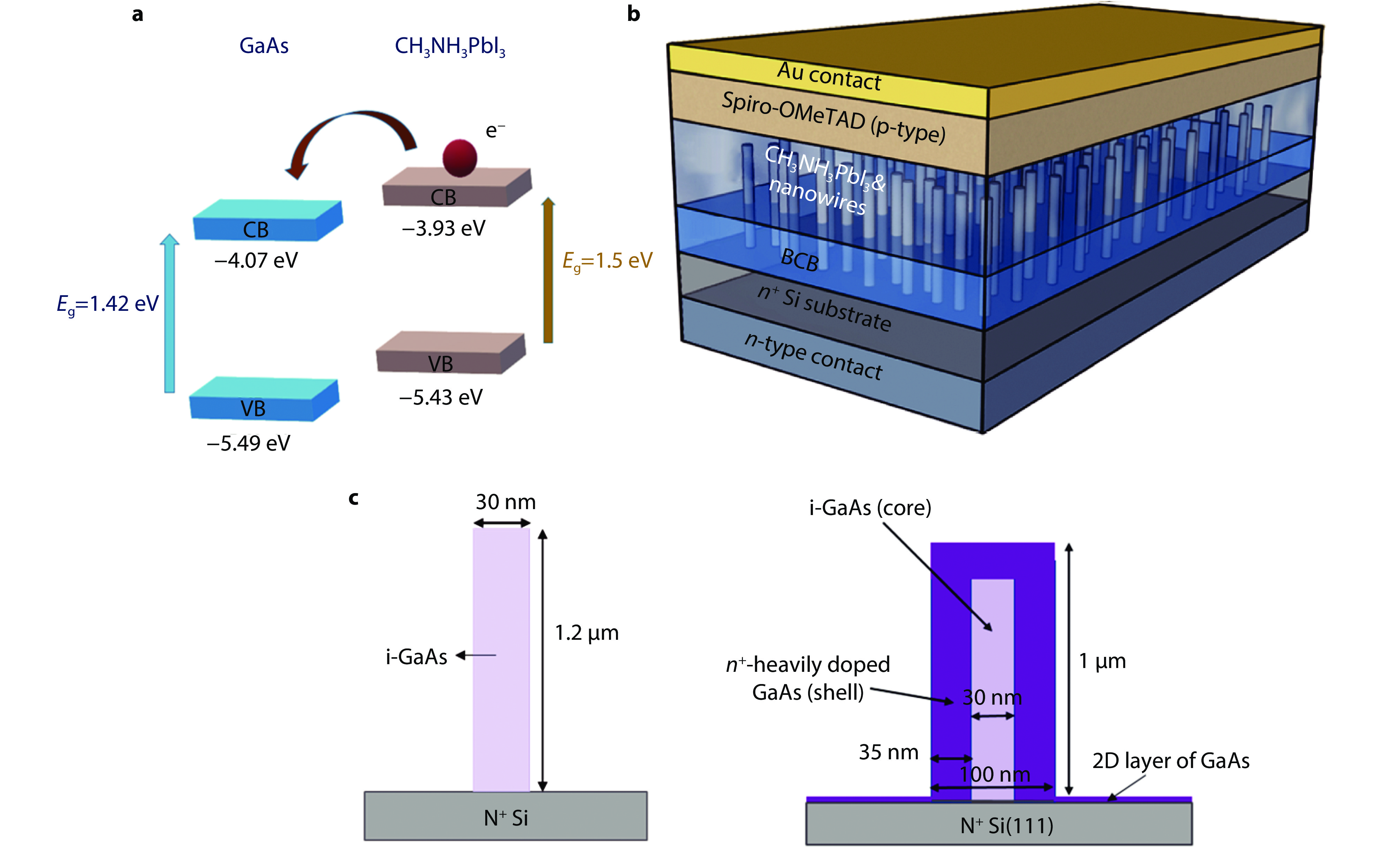
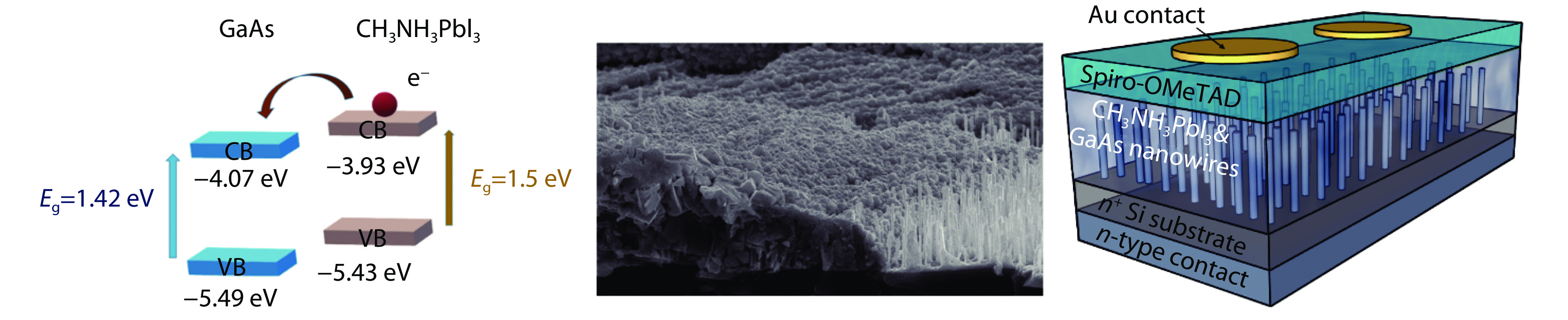
Figure 1.
a Schematic representation of energy levels for GaAs and CH3NH3PbI3 perovskite, indicating favorable band alignment for electron transport between CH3NH3PbI3 and GaAs. b The device architecture. c Schematic representation of the composition of the GaAs nanowires in intrinsic and doped variants, respectively. In the case of doped nanowires, a thin 2D layer of GaAs is also deposited on the substrate during the deposition of the GaAs shell.
-
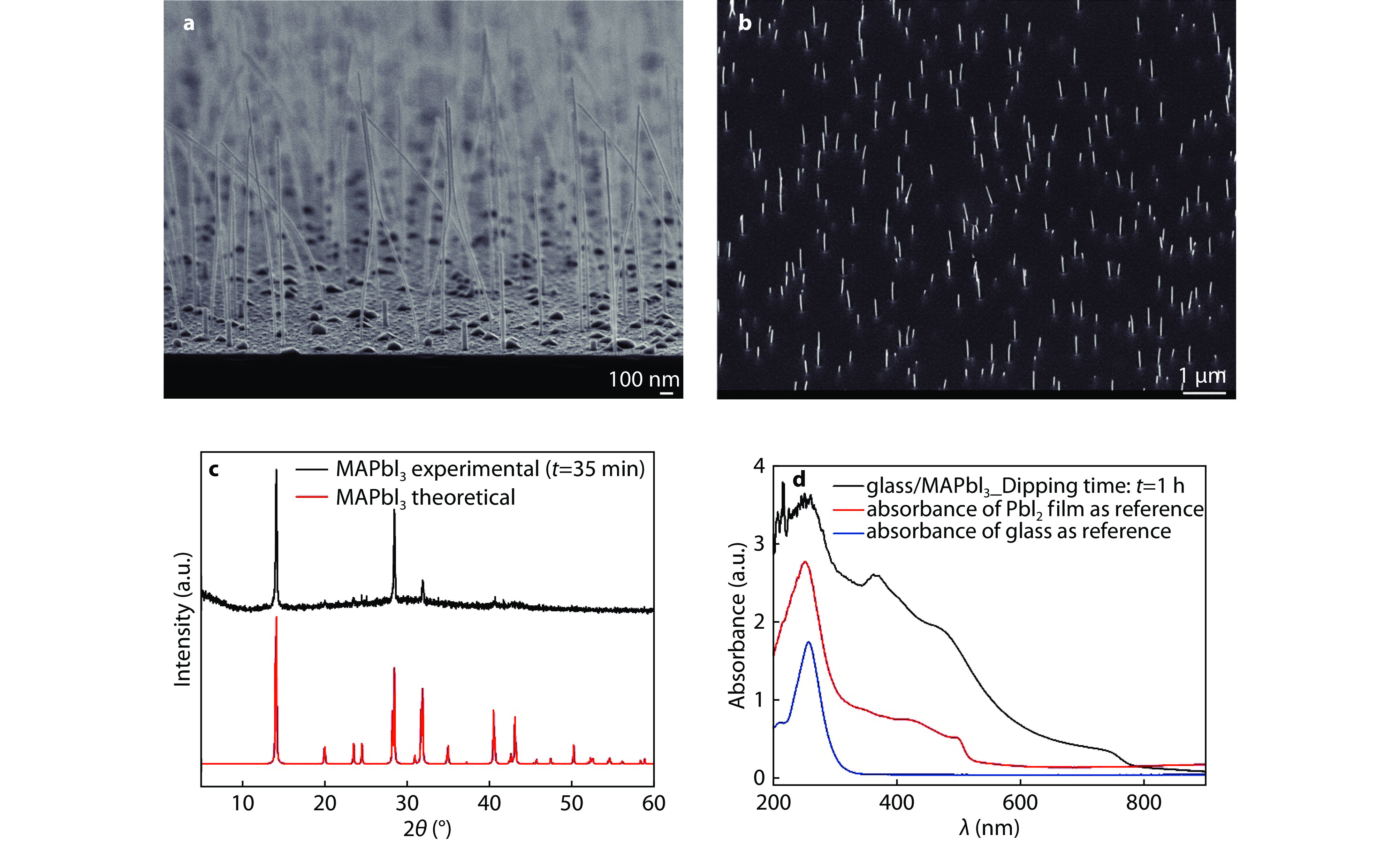
Figure 3.
a, b SEM images of the as-grown GaAs NWs in cross-plane and near-vertical view, for undoped NW structures (see NW composition in figure 1c), before and after the deposition of BCB layer on nanowire structures, respectively. c XRD pattern of the CH3NH3PbI3 perovskite film prepared on a glass substrate by the modified two-step sequential deposition method in comparison with the theoretical XRD pattern. Strong preferential orientation of the crystals is observed. d Absorption spectrum of the CH3NH3PbI3 perovskite film on soda lime glass.
-
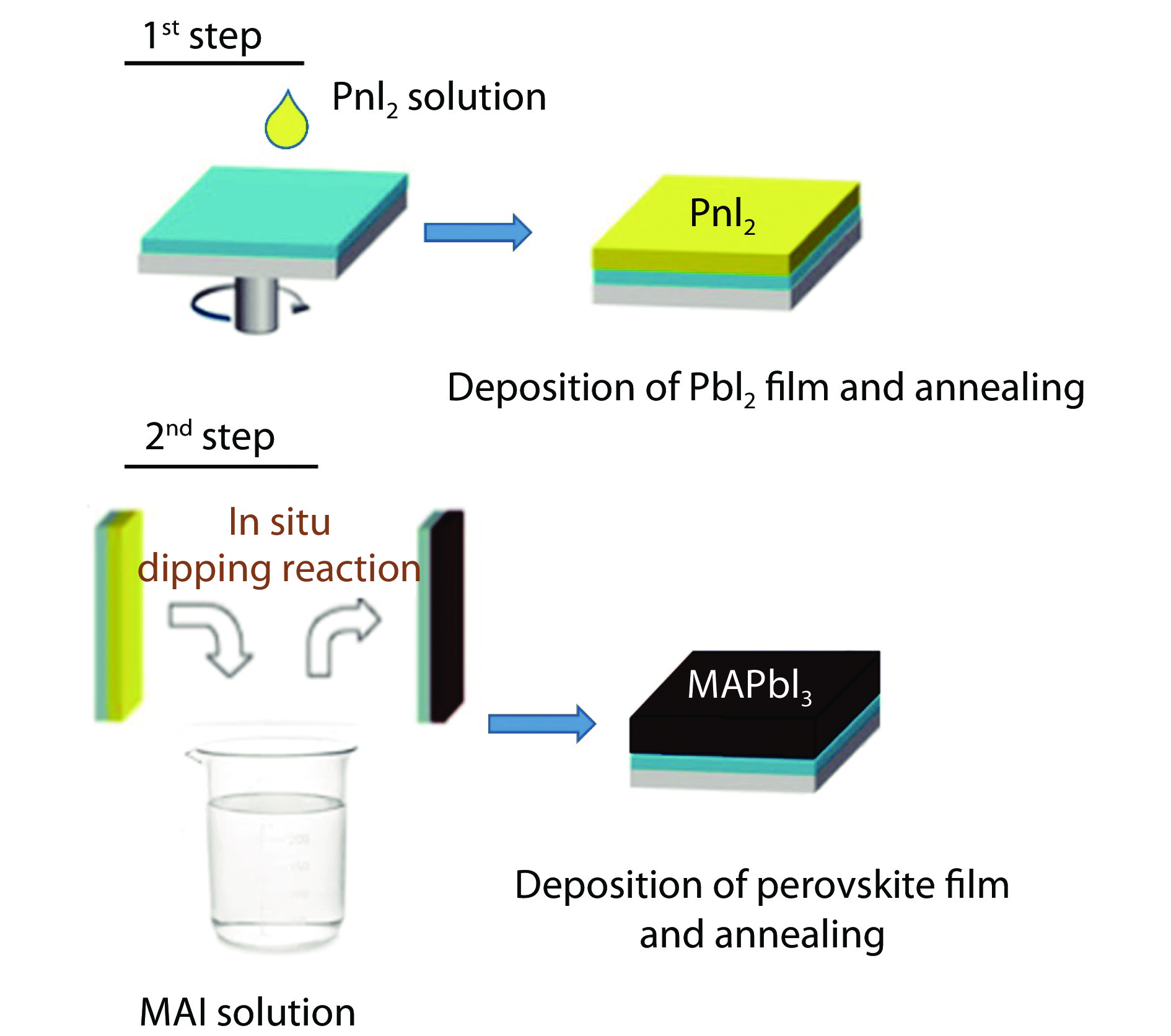
Figure 2.
Schematic representation of the two-step sequential deposition method, that was used for the deposition of perovskite layer.
-
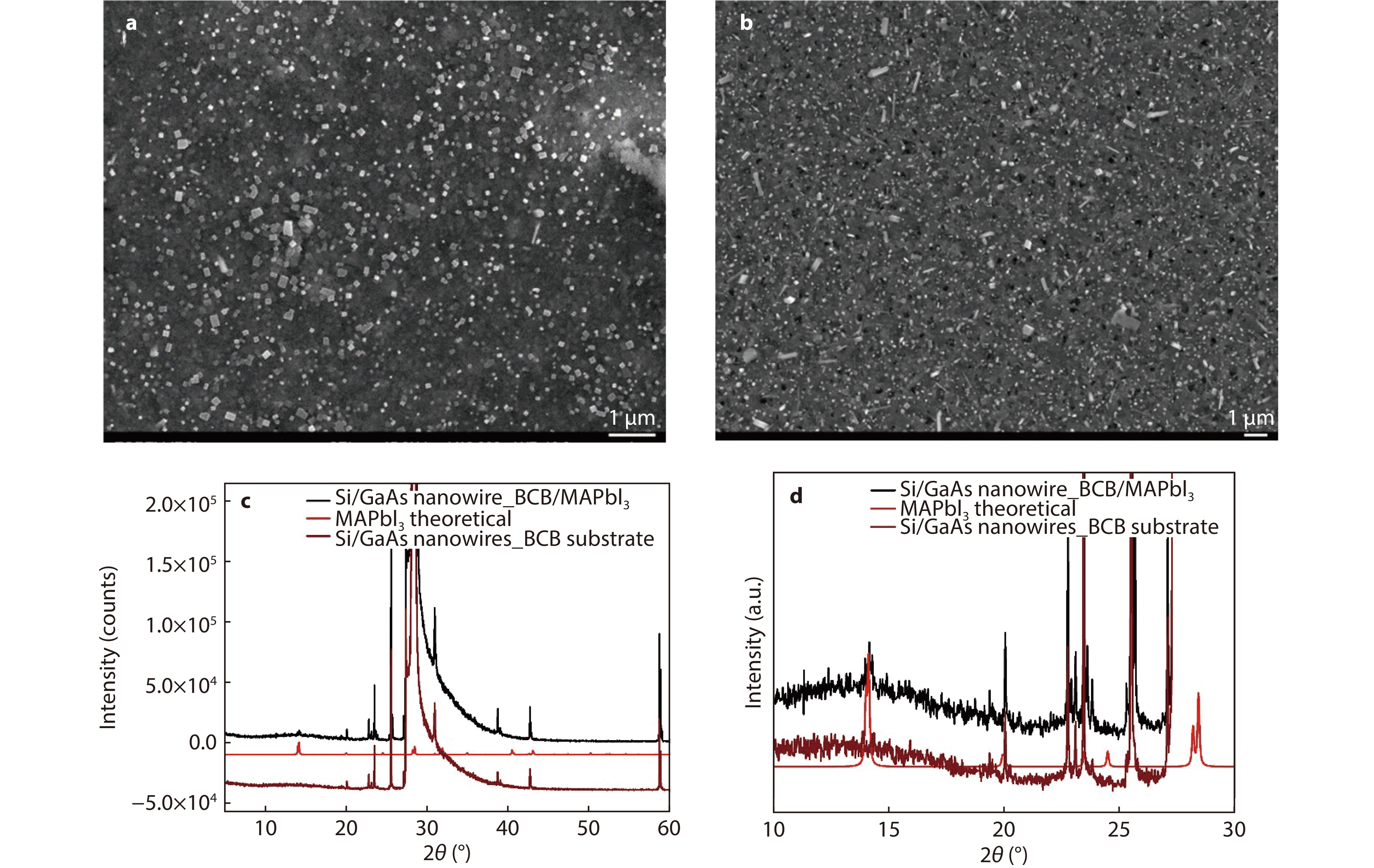
Figure 4.
a, b SEM images of the CH3NH3PbI3/GaAs NW heterostructure for two different perovskite deposition conditions (30 min and 60 min dipping time, respectively). c, d XRD pattern of the CH3NH3PbI3/GaAs NW heterostructure indicating the formation of crystalline perovskite on top of the nanowires, evidenced by the reflection at ~ 14°. The overarching peak at 2θ = 29° results from the (111)-oriented Si substrate.
-
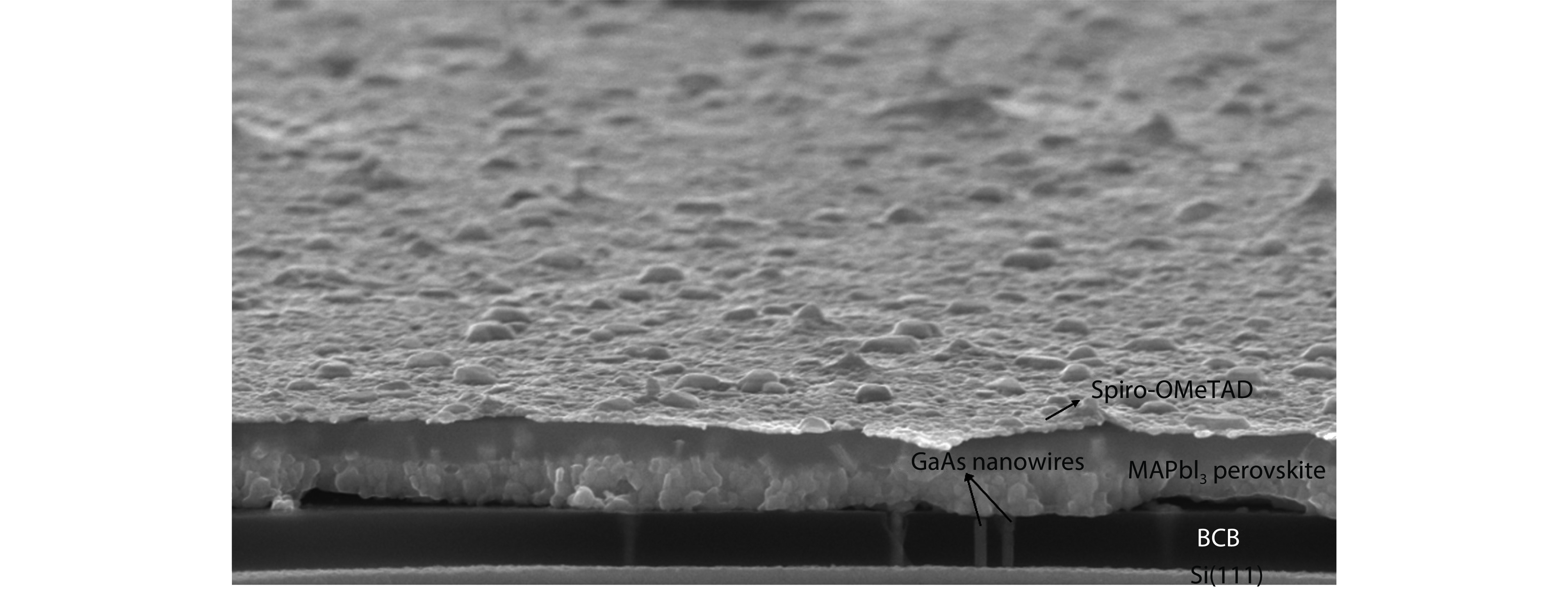
Figure 5.
SEM image in cross-section for the diode device, in case of 1 h dipping time. The (circular) electrode layer is not included in the SEM image. In the SEM image, homogeneous deposition of perovskite layer on nanowire structures is revealed. GaAs nanowires are not apparent through the perovskite layer which is attributed to non-efficient cleaving of the diode device for taking the SEM image in cross-section.
-
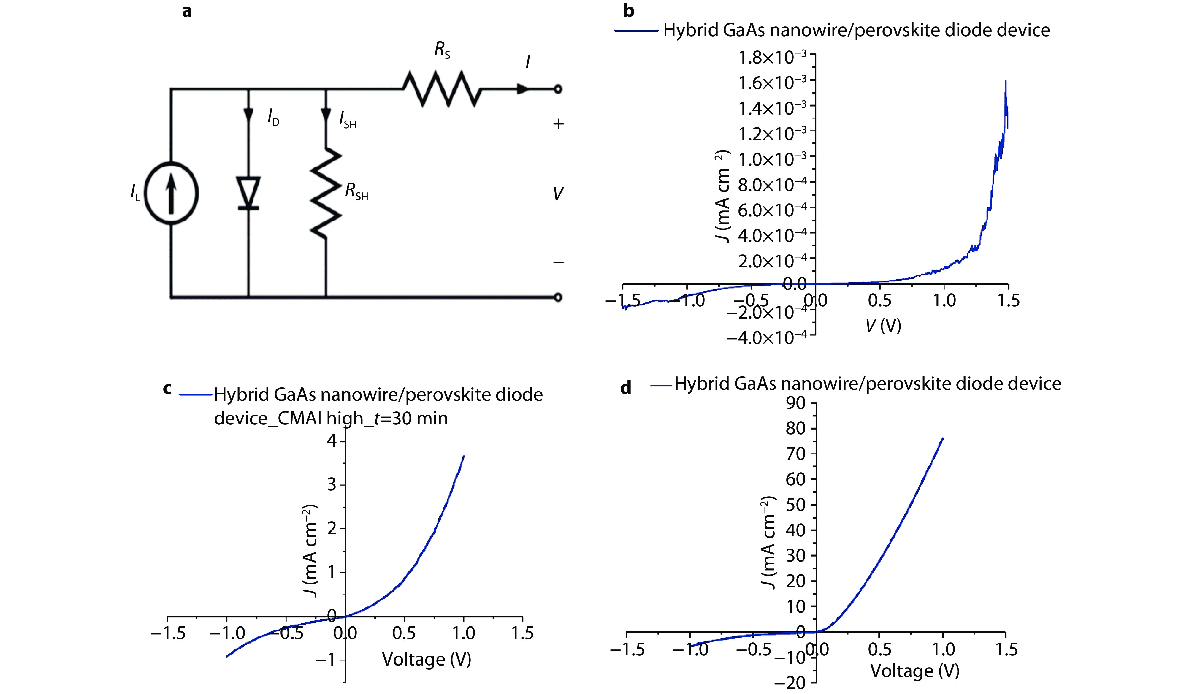
Figure 6.
a Schematic representation of the equivalent electrical circuit of the CH3NH3PbI3/GaAs NWs heterojunction. b I-V characteristics of the diode between pristine GaAs NWs and CH3NH3PbI3. c, d I-V characteristics of the diode between doped GaAs NWs and CH3NH3PbI3 for two different perovskite deposition conditions (30 min and 60 min dipping times, respectively).