| Citation: | Fudong Zhang, Di Wu, Jiaqing He. The Roles of Grain Boundaries in Thermoelectric Transports. Materials Lab 2022, 1, 220012. doi: 10.54227/mlab.20220012 |
The Roles of Grain Boundaries in Thermoelectric Transports
Published as part of the Virtual Special Issue "Mercouri G. Kanatzidis at 65"
-
Abstract
Grain boundary scattering was long recognized and widely utilized to regulate the transports of charge carriers and phonons in thermoelectric materials; nevertheless, the understanding of grain boundaries in lots of literatures seems somewhat lopsided and way too simplified, without distinguishing the exact microstructural characters for each individual case. In this perspective, we first review the well-known functions of grain boundaries on the electrical and thermal transport properties based on some representative thermoelectric series. Next, we try to deepen the understanding of the roles of grain boundaries in the following two aspects: (1) whether the grain boundaries are large-angle or small-angle ones, and what the difference between them in affecting electrical/thermal performance is; (2) whether the grain boundaries are clean and sharp as lattice discontinuity defects, if not, how can the grain boundaries as an individual phase affect the thermoelectric transports. At last, we suggest that further investigations engaging more detailed microstructural information of grain boundaries are urgently necessary in order to better realize a positive trade-off between lattice thermal conductivity and electrical power factor for an overall enhanced thermoelectric performance.
-
Keywords:
- grain boundary angle /
- grain boundary phase.
-

-
References
1. D. Wu, L.-D. Zhao, F. Zheng, L. Jin, M. G. Kanatzidis, J. He, Adv. Mater., 2016, 28, 2737 2. B. Qin, L.-D. Zhao, Mat. Lab, 2022, 1, 220004 3. N. Dragoe, Mat. Lab, 2022, 1, 220001 4. T. Zhu, Y. Liu, C. Fu, J. P. Heremans, J. G. Snyder, X. Zhao, Adv. Mater., 2017, 29, 1605884 5. C. Gayner, Y. Amouyal, Adv. Funct. Mater., 2020, 30, 1901789 6. G. Tan, L. D. Zhao, M. G. Kanatzidis, Chem. Rev., 2016, 116, 12123 7. D. Wu, L. Xie, X. Xu, J. He, Adv. Funct. Mater., 2019, 29, 1806613 8. N. K. Singh, A. Kashyap, A. Soni, Appl. Phys. Lett., 2021, 119, 223903 9. N. K. Singh, A. Soni, Appl. Phys. Lett., 2020, 117, 123901 10. Y. Zheng, T. J. Slade, L. Hu, X. Y. Tan, Y. Luo, Z. Z. Luo, J. Xu, Q. Yan, M. G. Kanatzidis, Chem. Soc. Rev., 2021, 50, 9022 11. G. Chen, T. Zeng, T. Borca-Tasciuc and D. Song, Mater. Sci. Eng. A, 2000, 292, 155 12. P. Das, S. Bathula, S. Gollapudi, Nano Express, 2020, 1, 020036 13. B. Poudel, Q. Hao, Y. Ma, Y. Lan, A. Minnich, B. Yu, X. Yan, D. Wang, A. Muto, D. Vashaee, X. Chen, J. Liu, M. S. Dresselhaus, G. Chen, Z. Ren, Science, 2008, 320, 634 14. M. S. Kim, W. J. Lee, K. H. Cho, J. P. Ahn, Y. M. Sung, ACS Nano., 2016, 10, 7197 15. A. Soni, Y. Zhao, L. Yu, M. K. Aik, M. S. Dresselhaus, Q. Xiong, Nano Lett., 2012, 12, 1203 16. S. Kim, K. H. Lee, H. A Mun, H. S. Kim, S. W. Hwang, J. W. Roh, D. J. Yang, W. H. Shin, X. S. Li, Y. H. Lee, G. J. Snyder, S. W. Kim, Science, 2015, 348, 109 17. X. Meng, Z. Liu, B. Cui, D. Qin, H. Geng, W. Cai, L. Fu, J. He, Z. Ren, J. Sui, Adv. Energy Mater., 2017, 7, 1602582 18. L. Yang, Z. G. Chen, G. Han, M. Hong, Y. Zou, J. Zou, Nano Energy, 2015, 16, 367 19. P. Zong, R. Hanus, M. Dylla, Y. Tang, J. Liao, Q. Zhang, G. J. Snyder, L. Chen, Energy Environ. Sci., 2017, 10, 183 20. W. Xie, X. Tang, Y. Yan, Q. Zhang, T. M. Tritt, J. Appl. Phys., 2009, 105, 113713 21. X. Yan, B. Poudel, Y. Ma, W. S. Liu, G. Joshi, H. Wang, Y. Lan, D. Wang, G. Chen, Z. F. Ren, Nano Lett., 2010, 10, 3373 22. Y. Zheng, Q. Zhang, X. Su, H. Xie, S. Shu, T. Chen, G. Tan, Y. Yan, X. Tang, C. Uher, G. J. Snyder, Adv. Energy Mater., 2015, 5, 1401391 23. T. J. Slade, T. P. Bailey, J. A. Grovogui, X. Hua, X. Zhang, J. J. Kuo, I. Hadar, G. J. Snyder, C. Wolverton, V. P. Dravid, C. Uher, M. G. Kanatzidis, Adv. Energy Mater., 2019, 9, 1901377 24. Y. Wu, F. Liu, Q. Zhang, T. Zhu, K. Xia, X. Zhao, J. Mater. Chem. A, 2020, 8, 8455 25. T. J. Slade, J. A. Grovogui, J. Kuo, S. Anand, T. P. Bailey, M. Wood, C. Uher, G. J. Snyder, V. P. Dravid, M. G. Kanatzidis, Energy Environ. Sci., 2020, 13, 1509 26. Q. Qiu, Y. Liu, K. Xia, T. Fang, J. Yu, X. Zhao, T. Zhu, Adv. Energy Mater., 2019, 9, 1803447 27. J. H. Bahk, A. Shakouri, Phys. Rev. B, 2016, 93, 165209 28. J. Martin, L. Wang, L. Chen, G. S. Nolas, Phys. Rev. B, 2009, 79, 115311 29. T. M. Roberts, M. E. Mauel, M. C. Abler, B. K. Makansi, Rev. Sci. Instrum., 2015, 86, 083510 30. H. Mun, K. H. Lee, S. J. Yoo, H. S. Kim, J. Jeong, S. H. Oh, G. J. Snyder, Y. H. Lee, Y. M. Kim, S. W. Kim, Acta Mater., 2018, 159, 266 31. S. Li, Y. Liu, F. Liu, D. He, J. He, J. Luo, Y. Xiao, F. Pan, Nano Energy, 2018, 49, 257 32. Y. Yu, D. S. He, S. Zhang, O. C. Mirédin, T. Schwarz, A. Stoffers, X. Y. Wang, S. Zheng, B. Zhu, C. Scheu, D. Wu, J. Q. He, M. Wuttig, Z. Y. Huang, F. Q. Zu, Nano Energy, 2017, 37, 203 33. J. Y. Hwang, J. Kim, H. S. Kim, S. Kim, K. H. Lee, S. W. Kim, Adv. Energy Mater., 2018, 8, 1800065 34. J. J. Kuo, M. Wood, T. J. Slade, M. G. Kanatzidis, G. J. Snyder, Energy Environ. Sci., 2020, 13, 1250 35. S. Wang, X. Lu, A. Negi, J. He, K. Kim, H. Shao, P. Jiang, J. Liu, Q. Hao, Eng. Sci., 2022, 17, 45 36. J. J. Kuo, Y. Yu, S. D. Kang, O. C. Mirédin, M. Wuttig, G. J. Snyder, Adv. Mater, Adv. Mater.Interfaces, 2019, 6, 1900429 37. J. J. Kuo, S. D. Kang, K. Imasato, H. Tamaki, S. Ohno, T. Kanno, G. J. Snyder, Energy Environ. Sci., 2018, 11, 429 38. A. Soni, Y. Shen, M. Yin, Y. Zhao, L. Yu, X. Hu, Z. Dong, K. A. Khor, M. S. Dresselhaus, Q. Xiong, Nano Lett., 2012, 12, 4305 -
Rights and permissions
This is an open access article under the terms of the Creative Commons Attribution License, which permits use, distribution and reproduction in any medium, provided the original work is properly cited.
Information
Article Metrics
-
Figure 1.
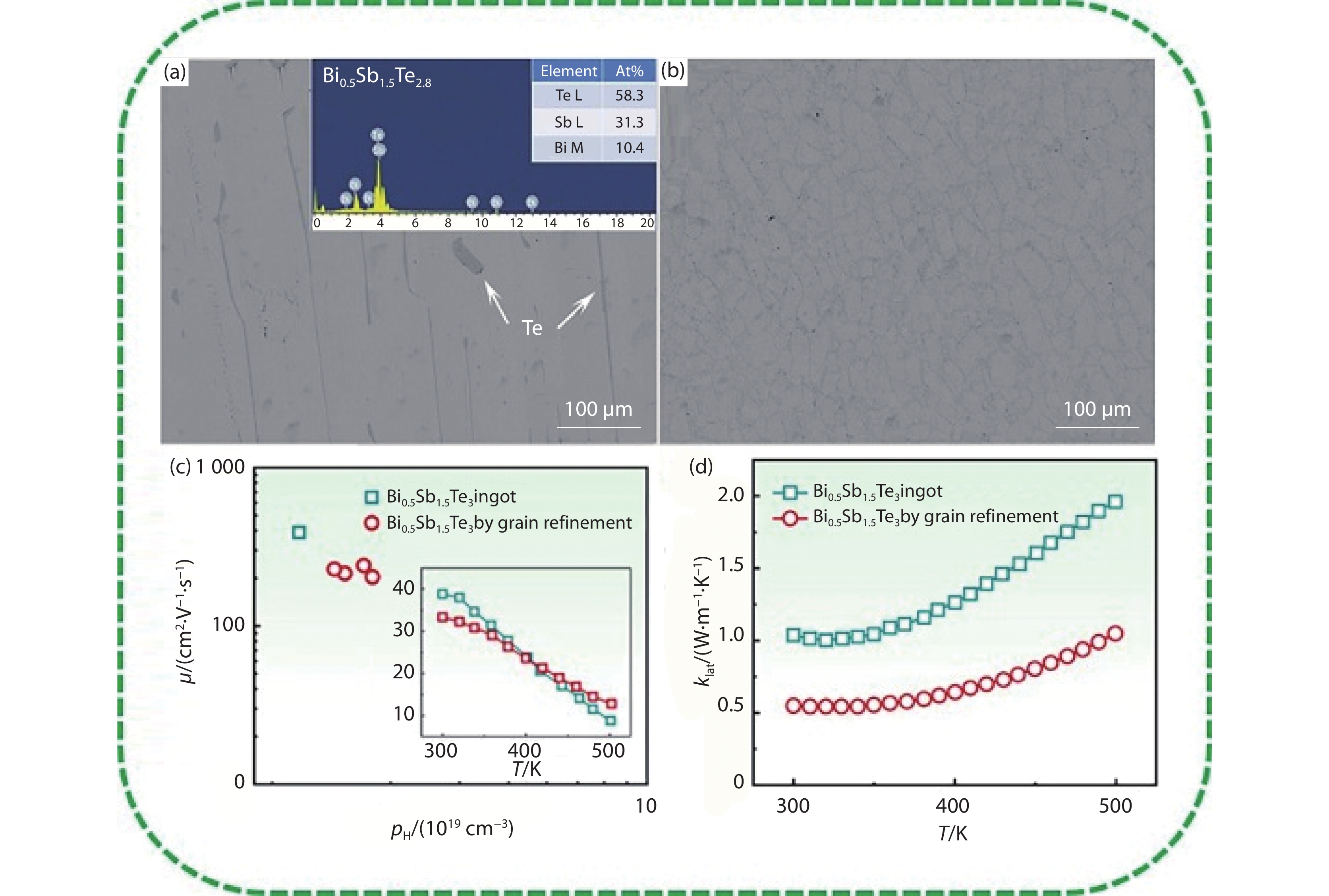
(a)(b) Comparison of BSE images between rough grains in an as-cast ingot and refined grain in a MS sample of the same Bi0.5Sb1.5Te3 composition. Reproduced with permission.[22] Copyright 2014 Wiley-VCH. (c) carrier mobility and PF, (d) T dependence κlat of Bi0.5Sb1.5Te3 ingot and mechanically robust polycrystal by grain refinement [22].
-
Figure 2.
Low-angle grain boundaries. (a)-(e) Periodic Moiré patterns at LAGBs and FFT images of adjacent grains crossing a tilt-type GB. Reproduced with permission.[16] Copyright 2015 American Association for the Advancement of Science. (f)(g) Selected electrical and thermal transport properties of S-MS sample with HAGBs and Te-MS sample with LAGBs[16]. (h) A high-resolution LAGB in Bi0.5Sb1.5Te3 alloy, (i)-(j) GPA mappings, and (k) corresponding FFT images. Reproduced with permission.[32] Copyright 2017 Elsevier.
-
Figure 3.
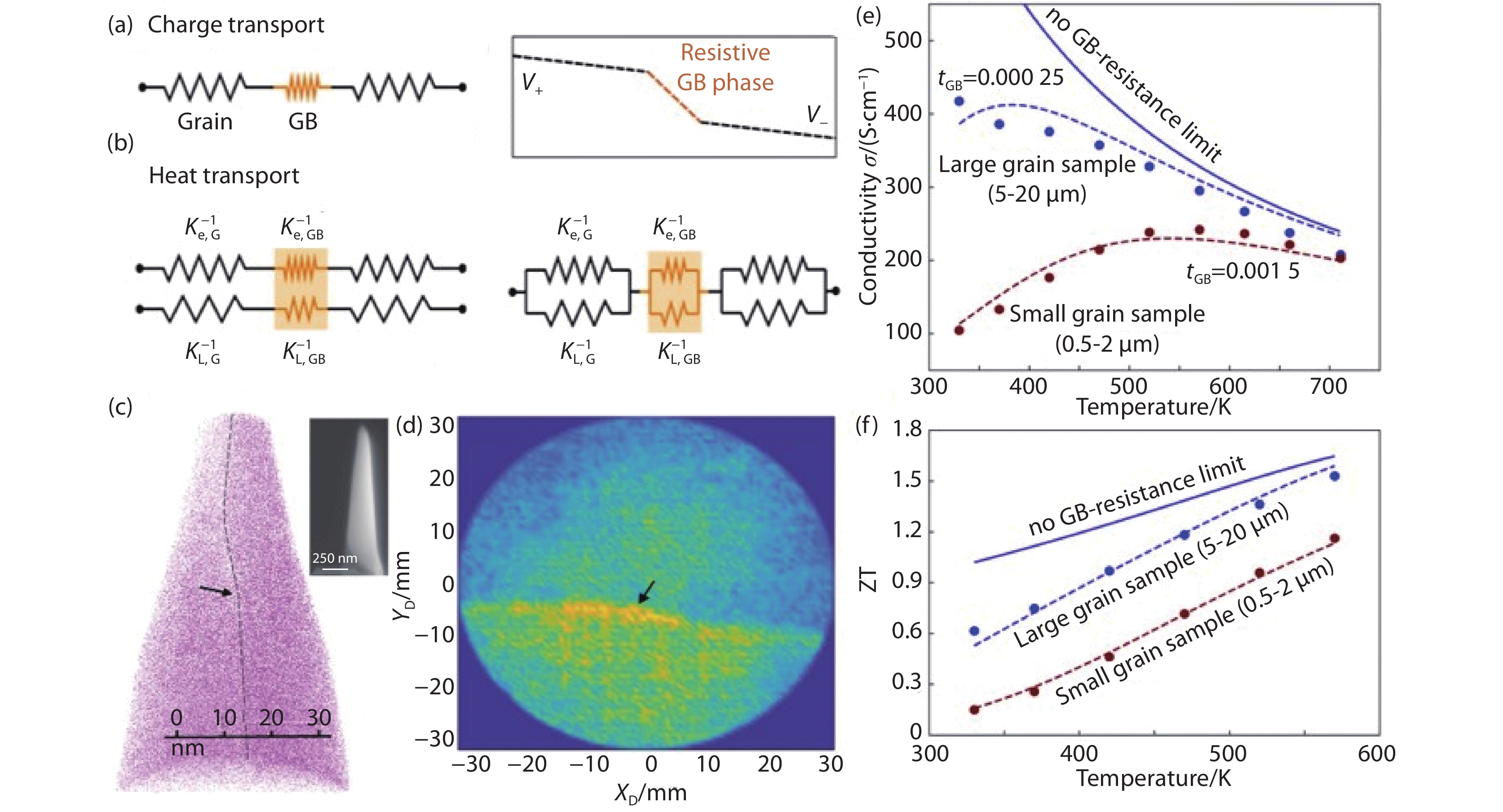
(a) Equivalent circuits for treating thermal and electrical resistance of grain boundaries. (b) Electrical and thermal transports in conventional use of the Wiedemann-Franz law (Fig. 3(b)-left) and when considering thermal and electrical resistance of grain boundaries in a two-phase model (Fig. 3(b)-right). Reproduced with permission.[34] Copyright 2020 Royal Society of Chemistry. (c)(d) 3D reconstruction of the atom distribution and projected atom density map in n-type Mg3Sb2 by Atom Probe Tomography (APT), the upper-right inset is a scanning electron microscope image. Reproduced with permission.[36] Copyright 2019 Wiley-VCH. (e) Scheme of thermally activated conduction behavior diminishing with increased grain size in Mg3.2Sb1.5Bi0.49Te0.01. (f) Upper limit of the figure-of-merit ZT with different grain size. Reproduced with permission.[37] Copyright 2018 Royal Society of Chemistry.

 Fudong Zhang is currently a Ph.D. candidate in School of Materials Science and Engineering, Shaanxi Normal University. His primary research interest is focused on Bi2Te3–based thermoelectric compounds, specifically, the sample synthesis, characterization and mechanism of thermoelectric transport.
  Di Wu joined School of Materials Science and Engineering of Shaanxi Normal University in 2017, after spending four years in Southern University of Science and Technology as a research assistance professor. His researches currently focus on interrelation between physical properties and microstructures in functional materials, such as thermoelectric materials and dielectric/ferroelectric ceramics.
  Jiaqing He is a Chair professor at Southern University of Science and Technology (SUSTech). He received his joint Ph.D. degree in physics from both Juelich Research Center and Wuhan University in 2004. He was a post-doctor at Brookhaven National Laboratory (2004–2008), research associate (2008– 2010) and research assistant professor (2010–2012) at Northwestern University, and a professor at Xi'an Jiaotong University (2012–2013) and SUSTech (2013-2019). His research interests include transmission electron microscopy, thermoelectric materials, and structure and property relationship.
 DownLoad:

