| Citation: |
Weiting Xu, Shengxue Yang. Seeking Novel Low-symmetry 2D Materials with Strong In-plane Anisotropy. Materials Lab 2022, 1, 220033. doi: 10.54227/mlab.20220033

|
Seeking Novel Low-symmetry 2D Materials with Strong In-plane Anisotropy
Published as part of the Virtual Special Issue “Beihang University at 70”
-
Abstract
Low-symmetry 2D materials, such as black phosphorus (BP), ReS2,
etc. , usually exhibit unique characteristic of its in-plane anisotropy. Inspired by this, the searching for novel low-symmetry 2D materials beyond BP and ReS2 is essential for creating polarization dependent devices and will benefit the future explorations of heterojunction on low-symmetry 2D materials. This perspective reviews the research on structure, characterization and applications of low-symmetry 2D materials. -

-
Author Biographies
 Weiting Xu is currently a Ph.D. candidate under the supervision of Professor Shengxue Yang in the School of Materials Science and Engineering, Beihang University. She received her B.S. degree from Nanning Normal University in 2018 and her M.S. degree from Hunan University in 2021. Her research focuses on the synthesis of 2D materials and complex heterostructures, nanoelectronics.
  Shengxue Yang is currently a full professor of Beihang University. She received her Ph.D. degree in 2013 from Northeast Normal University. She was a postdoctoral fellow in the State Key Laboratory of Superlattice, Institute of Semiconductors, Chinese Academy of Sciences (2013–2015). Then, she was a visiting postdoctoral fellow at the University of California, Los Angeles with Prof. Xiangfeng Duan (2016–2017). She has authored over 50 peer-reviewed publications in international journals with an h-index of 30. Her research focuses on the synthesis, characterization, and device application of low-dimensional materials.
 -
References
1. L. Pi, C. Hu, W. Shen, L. Li, P. Luo, X. Hu, P. Chen, D. Li, Z. Li, X. Zhou, T. Zhai, Adv. Funct. Mater., 2021, 31, 2006774 2. Z. Shu, Q. Peng, P. Huang, Z. Xu, A. A. Suleiman, X. Zhang, X. Bai, X. Zhou, T. Zhai, Matter, 2020, 2, 977 3. H. Yuan, X. Liu, F. Afshinmanesh, W. Li, G. Xu, J. Sun, B. Lian, A. G. Curto, G. Ye, Y. Hikita, Z. Shen, S. C. Zhang, X. Chen, M. Brongersma, H. Y. Hwang, Y. Cui, Nat. Nanotechnol., 2015, 10, 707 4. R. Wang, F. Zhou, L. Lv, S. Zhou, Y. Yu, F. Zhuge, H. Li, L. Gan, T. Zhai, CCS Chem., 2019, 1, 268 5. Y. Zhang, H.-L. Yi, H.-P. Tan, ACS Photonics, 2018, 5, 3739 6. L. Li, W. Han, L. Pi, P. Niu, J. Han, C. Wang, B. Su, H. Li, J. Xiong, Y. Bando, T. Zhai, InfoMat., 2019, 1, 54 7. T. Low, R. Roldan, H. Wang, F. Xia, P. Avouris, L. M. Moreno, F. Guinea, Phys. Rev. Lett., 2014, 113, 106802 8. F. Xia, H. Wang, Y. Jia, Nat. Commun., 2014, 5, 4458 9. J. Qiao, X. Kong, Z. X. Hu, F. Yang, W. Ji, Nat. Commun., 2014, 5, 4475 10. H. Liu, A. T. Neal, Z. Zhu, Z. Luo, X. Xu, D. Tomanek, P. D. Ye, ACS Nano, 2014, 8, 4033 11. S. Yang, Y. Yang, M. Wu, C. Hu, W. Shen, Y. Gong, L. Huang, C. Jiang, Y. Zhang, P. M. Ajayan, Adv. Funct. Mater., 2018, 28, 1707379 12. S. Yang, C. Hu, M. Wu, W. Shen, S. Tongay, K. Wu, B. Wei, Z. Sun, C. Jiang, L. Huang, Z. Wang, ACS Nano, 2018, 12, 8798 13. S. Liu, Y. Chen, S. Yang, C. Jiang, Nano Res., 2022, 15, 1532 14. S. Yang, Y. Liu, M. Wu, L.-D. Zhao, Z. Lin, H.-c. Cheng, Y. Wang, C. Jiang, S.-H. Wei, L. Huang, Y. Huang, X. Duan, Nano Res., 2018, 11, 554 15. Y. Yang, S. C. Liu, X. Wang, Z. Li, Y. Zhang, G. Zhang, D. J. Xue, J. S. Hu, Adv. Funct. Mater., 2019, 29, 1900411 16. Y. Yang, S.-C. Liu, Y. Wang, M. Long, C.-M. Dai, S. Chen, B. Zhang, Z. Sun, Z. Sun, C. Hu, S. Zhang, L. Tong, G. Zhang, D.-J. Xue, J.-S. Hu, Adv. Optical Mater., 2019, 7, 1801311 17. Y. Yang, X. Wang, S. C. Liu, Z. Li, Z. Sun, C. Hu, D. J. Xue, G. Zhang, J. S. Hu, Adv. Sci., 2019, 6, 1801810 18. Y. Yang, S. C. Liu, Z. Li, D. J. Xue, J. S. Hu, Chem. Commun., 2021, 57, 565 19. Y. Yang, S. C. Liu, W. Yang, Z. Li, Y. Wang, X. Wang, S. Zhang, Y. Zhang, M. Long, G. Zhang, D. J. Xue, J. S. Hu, L. J. Wan, J. Am. Chem. Soc., 2018, 140, 4150 20. T. Zhang, Y. Wang, H. Li, F. Zhong, J. Shi, M. Wu, Z. Sun, W. Shen, B. Wei, W. Hu, X. Liu, L. Huang, C. Hu, Z. Wang, C. Jiang, S. Yang, Q. M. Zhang, Z. Qu, ACS Nano, 2019, 13, 11353 21. T. Zhang, Y. Zhang, M. Huang, B. Li, Y. Sun, Z. Qu, X. Duan, C. Jiang, S. Yang, Adv. Sci., 2022, 9, 2105483 22. Y. Liu, M. Wu, Z. Sun, S. Yang, C. Hu, L. Huang, W. Shen, B. Wei, Z. Wang, S. Yang, Y. Ye, Y. Li, C. Jiang, Nanoscale, 2019, 11, 23116 23. S. Yang, M. Wu, W. Shen, L. Huang, S. Tongay, K. Wu, B. Wei, Y. Qin, Z. Wang, C. Jiang, C. Hu, ACS Appl. Mater. Interfaces, 2019, 11, 3342 24. J. Dai, X. C. Zeng, Angew. Chem., 2015, 127, 7682 25. J. O. Island, R. Biele, M. Barawi, J. M. Clamagirand, J. R. Ares, C. Sanchez, H. S. van der Zant, I. J. Ferrer, R. D'Agosta, A. Castellanos-Gomez, Sci. Rep., 2016, 6, 22214 26. J. Shi, P. Yu, F. Liu, P. He, R. Wang, L. Qin, J. Zhou, X. Li, J. Zhou, X. Sui, S. Zhang, Y. Zhang, Q. Zhang, T. C. Sum, X. Qiu, Z. Liu, X. Liu, Adv. Mater., 2017, 29, 1701486 27. W. Xin, X. K. Li, X. L. He, B. W. Su, X. Q. Jiang, K. X. Huang, X. F. Zhou, Z. B. Liu, J. G. Tian, Adv. Mater., 2018, 30, 1704653 -
Rights and permissions
This is an open access article under the terms of the Creative Commons Attribution License, which permits use, distribution and reproduction in any medium, provided the original work is properly cited.
Figures(6)
Tables(1)
Information
Article Metrics
Export File
Citation
Weiting Xu, Shengxue Yang. Seeking Novel Low-symmetry 2D Materials with Strong In-plane Anisotropy. Materials Lab 2022, 1, 220033. doi: 10.54227/mlab.20220033
Format
Content
 DownLoad:

-
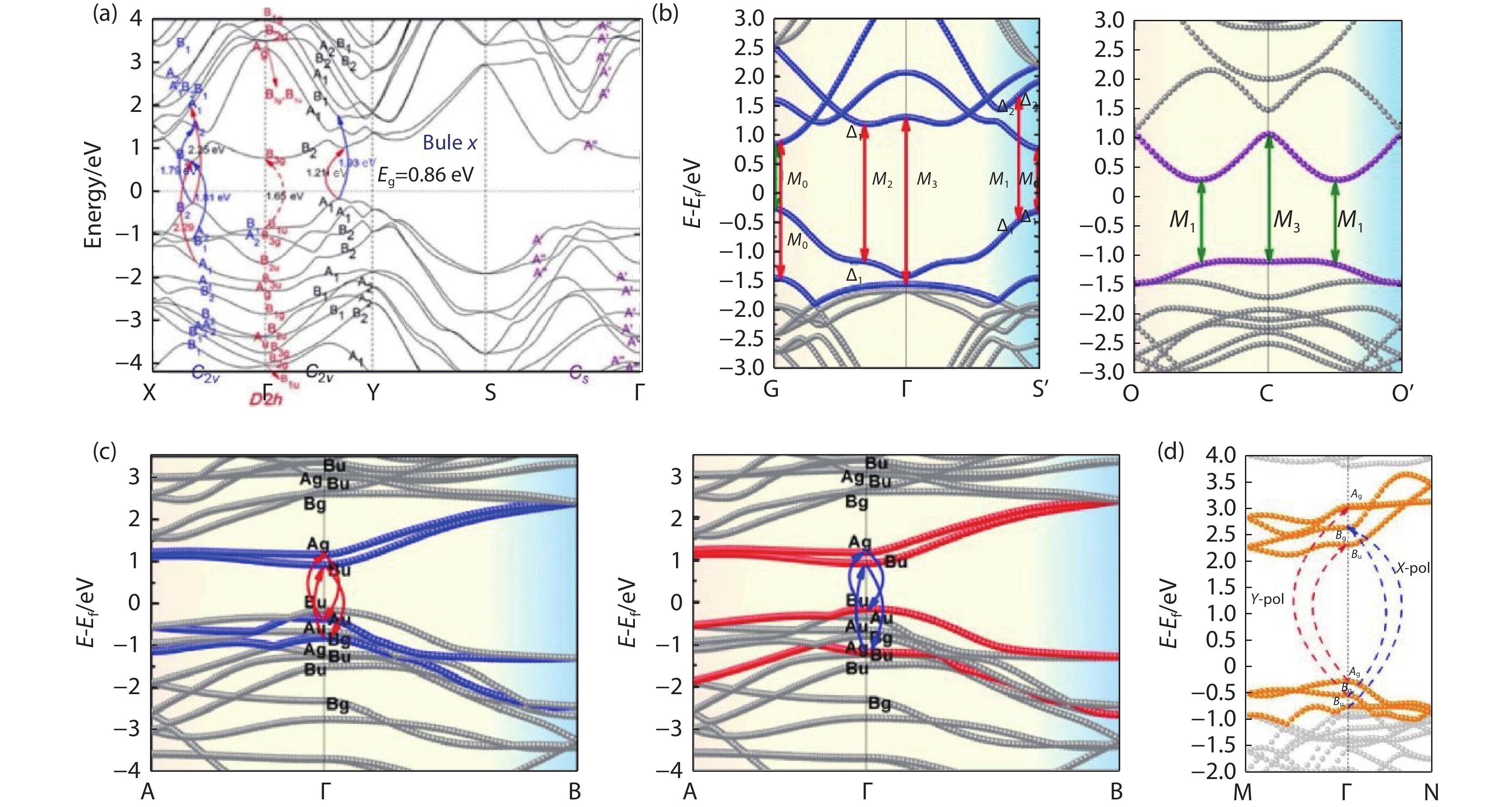
Figure 1.
Anisotropic band structure of low-symmetry 2D materials. (a) Band structure of SnSe[14]. Copyright 2017, Springer Nature. (b) Band structure of TlSe[12]. Copyright 2018, American Chemical Society. (c) Band structure of Nb(1−x)TixS3[23]. Copyright 2019, American Chemical Society. (d) Band structure of CrOCl[20]. Copyright 2019, American Chemical Society.
-
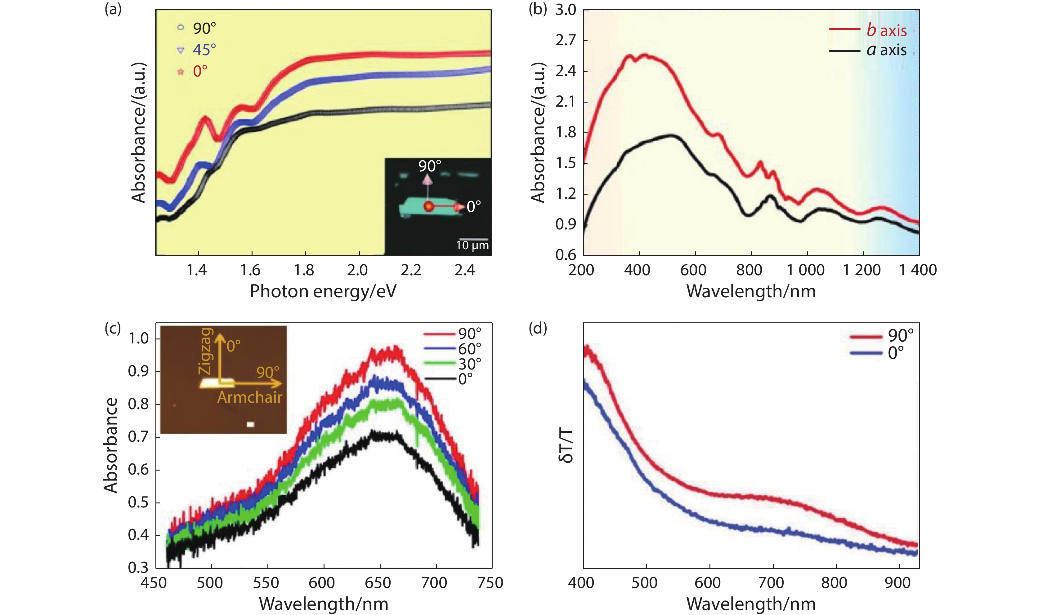
Figure 2.
Anisotropic optical absorption of low-symmetry 2D materials. (a) Anisotropic absorption spectra of TlSe. The polarization angle of 0° and 90° correspond to the zigzag and armchair directions, respectively[12]. Copyright 2018, American Chemical Society. (b) Anisotropic absorption spectra of Nb(1−x)TixS3. The b-axis and a-axis correspond to zigzag and armchair directions, respectively[23]. Copyright 2019, American Chemical Society. (c) Anisotropic absorption spectra of SnSe[14]. Copyright 2017, Springer Nature. (d) Anisotropic absorption spectra of Ge(1−x)SnxSe2. The polarization angle of 0° and 90° correspond to the zigzag and armchair directions, respectively[22]. Copyright 2019, RSC Pub.
-
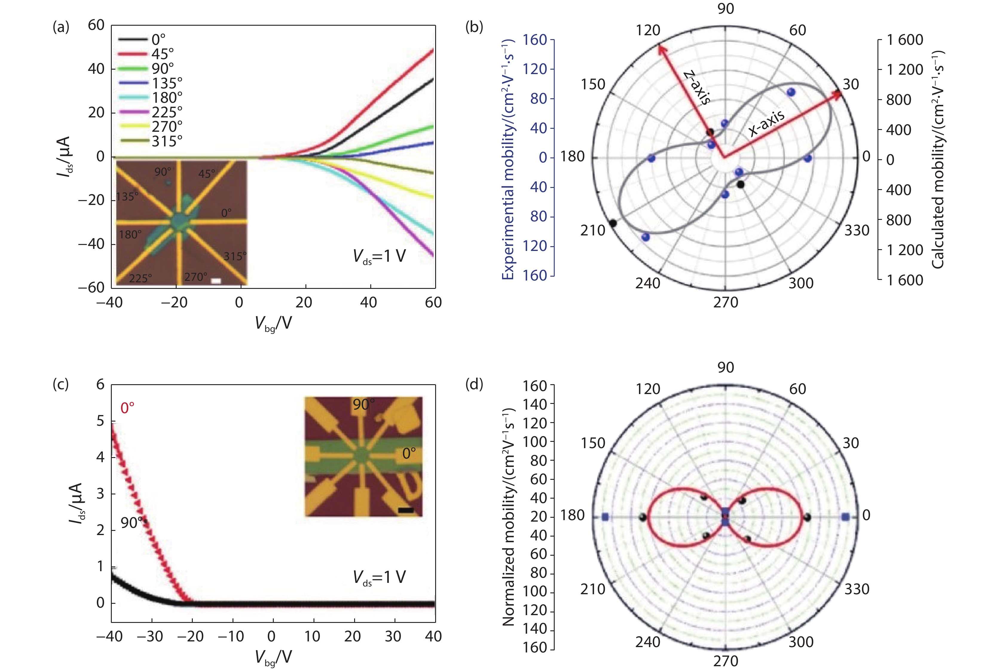
Figure 3.
Anisotropic electronic transport properties of SnSe and GeAs. (a) Transfer curves of anisotropic SnSe transistors. (b) Polar plot of normalized field-effect mobility for SnSe transistors[14]. Copyright 2017, Springer Nature. (c) Transfer curves of anisotropic GeAs transistors. (d) Polar plot of normalized field-effect mobility for GeAs transistors[11]. Copyright 2018, John Wiley and Sons.
-
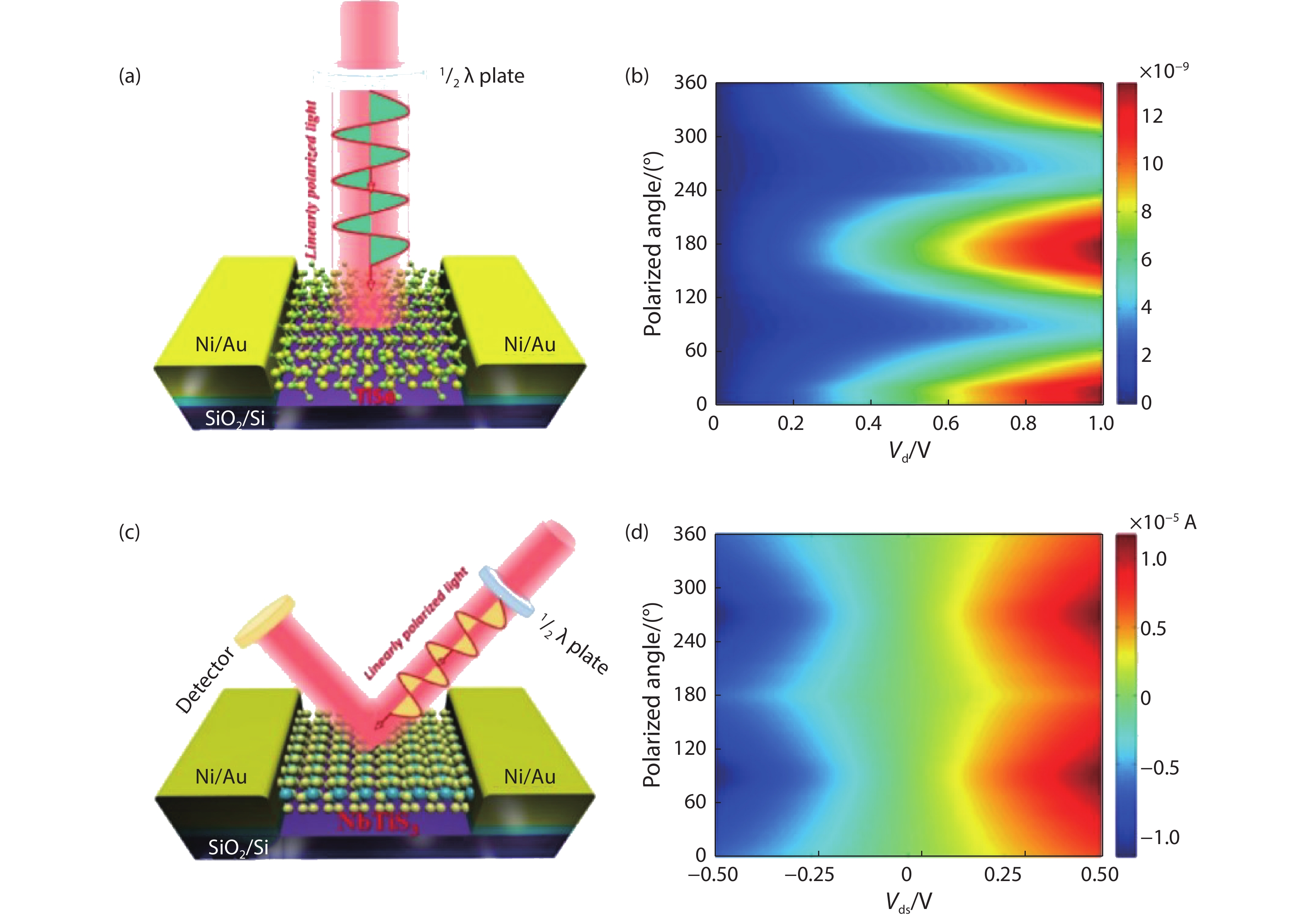
Figure 4.
Optoelectronics application of TlSe and Nb(1−x)TixS3. (a) Schematic diagram of TlSe photodetection device. (b) 2D colormap of anisotropic photocurrent of TlSe[12]. Copyright 2018, American Chemical Society. (c) Schematic diagram of Nb(1−x)TixS3 photodetection device. (d) 2D colormap of anisotropic photocurrent of Nb(1−x)TixS3[23]. Copyright 2019, American Chemical Society.
-
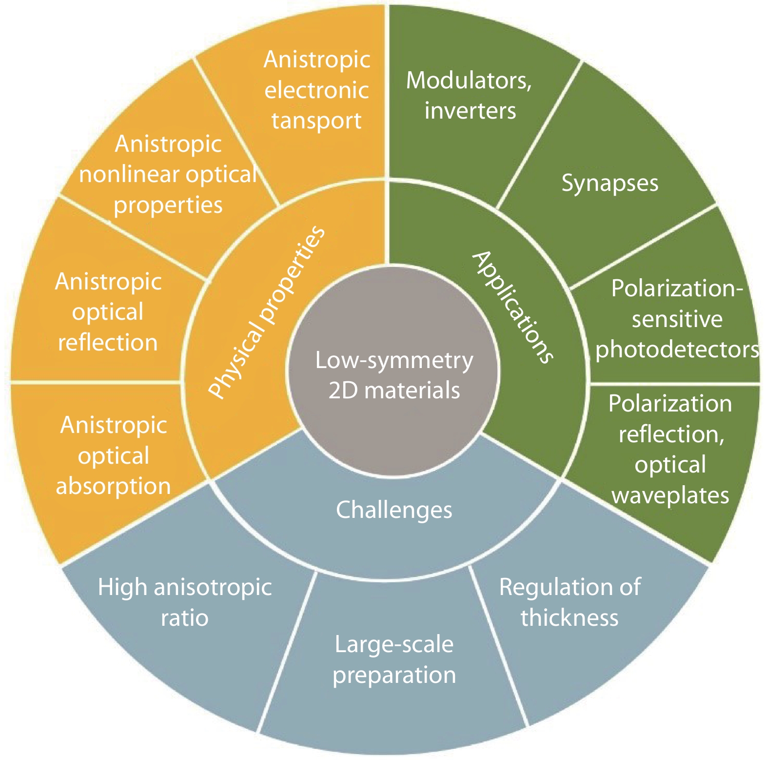
Figure 5.
Schematic of recent progress, future development and possible challenges in low-symmetry 2D materials.